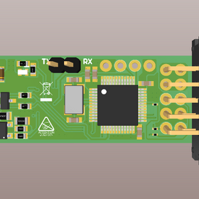
STLINK V2
1 Kasım 2024

The project includes the design of an in-circuit debugger and programmer for the STM8 and STM32 microcontrollers.
The STLINK V2 board is designed to handle debugging and programming tasks for STM8 and STM32 microcontrollers.
These critical functions include:
- Single-wire interface module (SWIM) and JTAG/serial wire debugging (SWD) interfaces.
The STM32F103C8T6 microprocessor is used as the processor.
It processes data received from peripherals and issues relevant commands.
The circuit is powered via Mini USB Type-B. This power must be distributed to the components in the circuit in a controlled manner. For this purpose, the circuit includes linear regulators with 5V to 3.3V reduction gears. These regulators eliminate voltage fluctuations in the circuit and provide pure DC power to the components in the circuit.
The circuit includes an oscillator (clock) circuit for use by the processor, a Reset button for manual reset, an STLINK communication terminal, an MCU programmer, and an STLINK output terminal.
The BOOTX pins are assigned "00" by default using pull-down resistors.
Power LEDs and Status LEDs have been added for control purposes.
USB 2.0 Type B TVS diodes protect against interference and voltage fluctuations.
All electronic components used in the project are:
- STM32F103C8T6, LQFP48
- 8MHz Crystal
- TVS Diode (SM712)
- PTC Fuse (0805)
- NPN Transistor (BC817-16, SOT-23)
- Tactile Switch (SMD)
- LM1117-3.3, SOT-223 Voltage Regulator
- Mini USB Type-B Connector
- Capacitors (all ceramic + tantalum)
- Resistors (all values)
- Jumper / Header connectors (2x1, 4x1, 5x2, etc.)
- Orange & Green/Red LED (0603)


